


The phono preamplifier amplifies the audio signal of a MC2.1 phono pickup with a sensitivity of 150![]() V to line level and also
equalizes the frequency response according to the RIAA deemphasis
curve (see [Hü97]). Additional equalization
according to the IEC deemphasis curve is not done as my turntable
does not produce significant drive noise and the electronics following
in the signal chain is able to handle all signals produced by the
MC pickup. Usually there is at least one highpass somewhere within
the signal chain between pickup and speaker which has enough suppression
of sub bass frequencies.
V to line level and also
equalizes the frequency response according to the RIAA deemphasis
curve (see [Hü97]). Additional equalization
according to the IEC deemphasis curve is not done as my turntable
does not produce significant drive noise and the electronics following
in the signal chain is able to handle all signals produced by the
MC pickup. Usually there is at least one highpass somewhere within
the signal chain between pickup and speaker which has enough suppression
of sub bass frequencies.
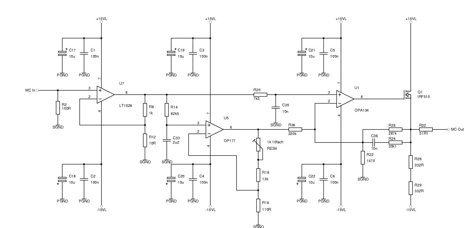
The preamplifier consists of several coupled stages (see the schematics ):
I choose two separate filters instead of one composite filter for the RIAA equalization because it is very difficult to construct a three pole filter where the poles are very close together and influences each other. If you look into the excellent paper in [Lip79] you'll understand what I mean.
Nowadays you can get extremely ultra low noise operational amplifiers which compare with transistor pairs regarding price but are more easily available. Furthermore a discrete amplifier using a transistor pair needs very high precision resistors and a very good stabilized supply voltage. Operational amplifiers on the other hand have all these parts built in. Examples of ultra low noise operational amplifiers are LT1028 by Linear Technology and AD797 by Analog Devices.
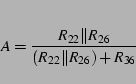
A none inverting amplifier is built with the feedback resistors
![]() and
and
![]() to get an amplification2.2 of about 40 dB. Usually I do not use feedback resistors with such
low resistance to prevent overloading the output of the operational
amplifier (it gets warm and does not sound very good). This case is
an exception because the input noise current of the operational amplifier
flows through
to get an amplification2.2 of about 40 dB. Usually I do not use feedback resistors with such
low resistance to prevent overloading the output of the operational
amplifier (it gets warm and does not sound very good). This case is
an exception because the input noise current of the operational amplifier
flows through ![]() which means that the output noise increases
with the resistance of
which means that the output noise increases
with the resistance of ![]() . Therefore its resistance should
be so low that its residual noise is small compared to the input voltage
noise of the amplifier.
. Therefore its resistance should
be so low that its residual noise is small compared to the input voltage
noise of the amplifier.
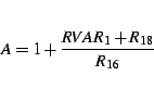
The input impedance is set by putting ![]() in parallel to the
input. Its value should be selected according to the specifications
of the MC pickup. Usually this is 100-150
in parallel to the
input. Its value should be selected according to the specifications
of the MC pickup. Usually this is 100-150![]() , for low output
MC pickups, high output pickups might need up to 1000
, for low output
MC pickups, high output pickups might need up to 1000![]() (check
the owner's manual). I chose
(check
the owner's manual). I chose
![]() .
.
This means that the none inverting input sees a source impedance of
![]() and the inverting input of
and the inverting input of
![]() .
As the input offset current (which is relatively high) flows through
both input impedances the imbalance leads to an additional input offset
voltage which is then amplified by 40 dB. Usually this can be prevented
by adding an additional resistor at the inverting input to recreate
the balance. I did not do this because the input noise current also
flows through this additional resistor, thereby adding unwanted voltage
noise. The resulting offset voltage of the first stage is later eliminated
by the offset compensation circuit.
.
As the input offset current (which is relatively high) flows through
both input impedances the imbalance leads to an additional input offset
voltage which is then amplified by 40 dB. Usually this can be prevented
by adding an additional resistor at the inverting input to recreate
the balance. I did not do this because the input noise current also
flows through this additional resistor, thereby adding unwanted voltage
noise. The resulting offset voltage of the first stage is later eliminated
by the offset compensation circuit.
At some later time I replaced ![]() in one channel by the serial
connection of a 750
in one channel by the serial
connection of a 750![]() resistor and a 500
resistor and a 500![]() adjustable
resistor. This allows to balance pickups with unequal output voltage.
adjustable
resistor. This allows to balance pickups with unequal output voltage.
I chose a passive filter to realize the 75 ![]() s lowpass for the
following reasons:
s lowpass for the
following reasons:
The capacitor should be of the highest quality
both in precision and sound. The only choice is a styroflex capacitor,
which is available with 1% tolerance. The biggest value is just about
15nF. I chose ![]() which leads to a resitance of
which leads to a resitance of
![]() according to equation 2.1, and this part is available
with 1% tolerance. I got hold of a large bunch of 10nF capacitors
and used a capacitance meter to select two capacitors of equal value
(to improve channel balance) as close to the specification as possible.
according to equation 2.1, and this part is available
with 1% tolerance. I got hold of a large bunch of 10nF capacitors
and used a capacitance meter to select two capacitors of equal value
(to improve channel balance) as close to the specification as possible.
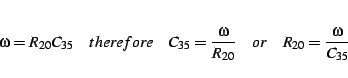
The second amplifer stage also serves as filter for the poles 318![]() s
and 3180
s
and 3180![]() s. It is possible to use a passive filter-however that
makes no sense as then the signal must be amplified much more which
leads to increased distortion, and this is not our target.
s. It is possible to use a passive filter-however that
makes no sense as then the signal must be amplified much more which
leads to increased distortion, and this is not our target.
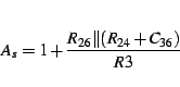
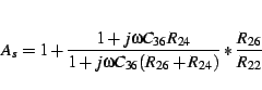
Therefore we need an active filter where the amplification is constant
between DC and 50,05 Hz, decreases by 6 dB/octave up to 500,5 Hz and
stays constant again for all higher frequencies. This is easily achieved
by adding the serial connection of resistor ![]() and capacitor
and capacitor
![]() parallel to resistor
parallel to resistor ![]() in the feedback loop. At
very low frequencies the impedance of
in the feedback loop. At
very low frequencies the impedance of ![]() is very high so that
the amplification depends on
is very high so that
the amplification depends on ![]() alone. At very high frequencies
the impedance of
alone. At very high frequencies
the impedance of ![]() is close to a short cut so that the amplification
depends on
is close to a short cut so that the amplification
depends on
![]() .
.
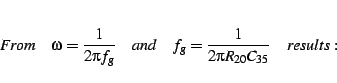
To be able to calculate the filter exactly we must find the transfer equation of the circuit. Having done this we can compare the coefficients of the amplification equation with those of the filter equation. Let's do this assuming an ideal operational amplifier (having infinite difference amplification and input impedance and zero output impedance)2.3.
The transfer equation of the active filter is:
 |
(2.4) | ||
 |
(2.5) | ||
| (2.6) |
 |
(2.10) | ||
 |
(2.11) | ||
| (2.12) |
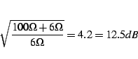
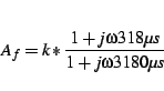
![[*]](/images/latex2html/crossref.png) .
.
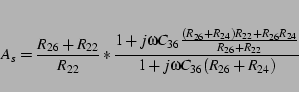
Subjective listening tests comparing the new preamplifier with my
old one2.5 by connecting the output of ![]() to the line level amplifier
showed that the sound of the new phono preamplifier was more clean,
had much more resolution and was much better at the frequency extremes,
but was also more cool, sterile and metallic and not that musical.
After countless tests I found a solution which added the missing characteristics:
a class A output stage within the feedback loop using a power Mosfet
(credits go to Nelson Pass).
to the line level amplifier
showed that the sound of the new phono preamplifier was more clean,
had much more resolution and was much better at the frequency extremes,
but was also more cool, sterile and metallic and not that musical.
After countless tests I found a solution which added the missing characteristics:
a class A output stage within the feedback loop using a power Mosfet
(credits go to Nelson Pass).
![]() is a source follower using the source resistance
is a source follower using the source resistance ![]() .
The quiescent current running through
.
The quiescent current running through ![]() is calculated according
to the equation
is calculated according
to the equation


The signal is coupled to both the line level amplifier and the tape
output via a serial resistor of ![]() each, because I use
each, because I use ![]() coax cables (RG58 / RG214U) both internal and external. This serial
resistor prevents reflections2.7.
coax cables (RG58 / RG214U) both internal and external. This serial
resistor prevents reflections2.7.
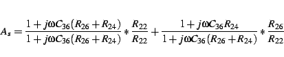
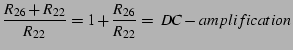
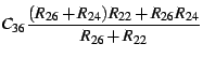
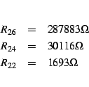
Both stages of the phono preamplifier together have a DC amplification
of approximately ![]() . Even when using the best precision operational
amplifiers money can buy today it is not possible to get rid of the
DC offset without reducing the DC amplification-which makes sense
anyway in a phono preamplifier. There are several possiblities how
to realize this:
. Even when using the best precision operational
amplifiers money can buy today it is not possible to get rid of the
DC offset without reducing the DC amplification-which makes sense
anyway in a phono preamplifier. There are several possiblities how
to realize this:
Approaching a corner frequency below 20 Hz requires a capacitance
of 4,7 ![]() F. Subjective listening tests using a capacitance of
6,8
F. Subjective listening tests using a capacitance of
6,8 ![]() F (leading to a corner frequency of 13 Hz) gave the impression
of reduced bass dynamic (punch) compared to a version with full DC
amplification. For a corner frequency of 1 Hz a capacitance of 82
F (leading to a corner frequency of 13 Hz) gave the impression
of reduced bass dynamic (punch) compared to a version with full DC
amplification. For a corner frequency of 1 Hz a capacitance of 82
![]() F is required, and a good one is very big in size and very expensive
too. You cannot use a cheap electrolytic capacitor as there is no
DC voltage applied which would lead to significant distortion.
F is required, and a good one is very big in size and very expensive
too. You cannot use a cheap electrolytic capacitor as there is no
DC voltage applied which would lead to significant distortion.
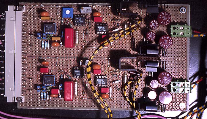
A top view of the printed circuit board
is in figure 2.2 on page .
![\includegraphics[%
height=0.95\textwidth]{phono_sp_tex.ps}](img2.png)
![\includegraphics[%
width=1.0\textwidth]{pre1-phono_tex.ps}](img69.png)